
- English
- Español
- Português
- русский
- Français
- 日本語
- Deutsch
- tiếng Việt
- Italiano
- Nederlands
- ภาษาไทย
- Polski
- 한국어
- Svenska
- magyar
- Malay
- বাংলা ভাষার
- Dansk
- Suomi
- हिन्दी
- Pilipino
- Türkçe
- Gaeilge
- العربية
- Indonesia
- Norsk
- تمل
- český
- ελληνικά
- український
- Javanese
- فارسی
- தமிழ்
- తెలుగు
- नेपाली
- Burmese
- български
- ລາວ
- Latine
- Қазақша
- Euskal
- Azərbaycan
- Slovenský jazyk
- Македонски
- Lietuvos
- Eesti Keel
- Română
- Slovenski
- मराठी
- Srpski језик
Kiina CVD SIC Valmistajat, toimittajat, tehdas


- View as

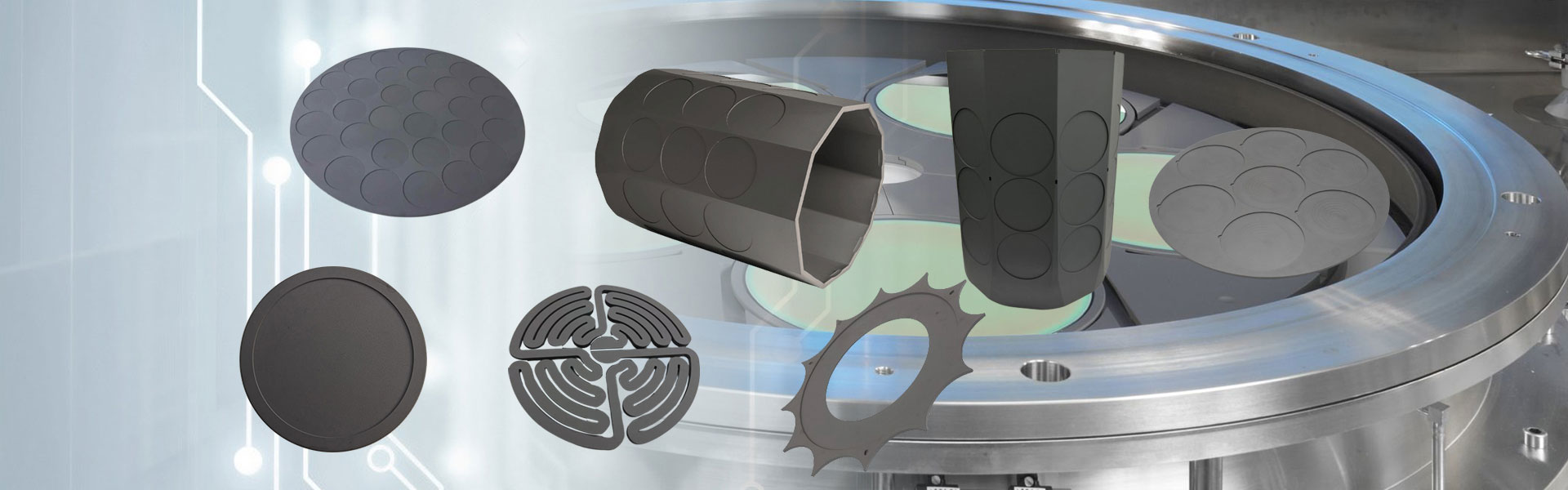
Kiinteät CVD SiC renkaat
Semicorex kiinteät CVD SiC -renkaat ovat tehokkaita renkaan muotoisia komponentteja, joita käytetään pääasiassa plasmaetsauslaitteiden reaktiokammioissa edistyneen puolijohdeteollisuuden alalla. Semicorex kiinteät CVD SiC -renkaat läpikäyvät tiukan materiaalin valinnan ja laadunvalvonnan, mikä tarjoaa vertaansa vailla olevan materiaalin puhtauden, poikkeuksellisen plasmakorroosionkestävyyden ja tasaisen toimintakyvyn.
Lue lisääLähetä kysely
Piikarbidin tarkennusrenkaat
Piikarbidin tarkennusrenkaat, tärkeimmät rengasosat, on erityisesti suunniteltu parantamaan kiekkojen etsauksen tasaisuutta ja vakautta puolijohdeplasmaetsauksessa. Ne tunnetaan erinomaisesta suorituskyvystään tasaisen plasman jakautumisen edistämisessä ja sähkökenttäympäristön optimoinnissa.
Lue lisääLähetä kysely
CVD SiC Suihkupäät
Semicorex CVD SiC -suihkupäät ovat erittäin puhtaita, tarkasti suunniteltuja komponentteja, jotka on suunniteltu edistyneen puolijohteiden valmistuksen CCP- ja ICP-etsausjärjestelmiin. Semicorexin valitseminen tarkoittaa luotettavien ratkaisujen hankkimista, joissa on erinomainen materiaalipuhtaus, koneistustarkkuus ja kestävyys vaativimpiin plasmaprosesseihin.*
Lue lisääLähetä kysely
Reunarenkaat
Semicorex Edge -renkaat luottavat johtavat puolijohteet ja OEM -valmistajat ympäri maailmaa. Tiukan laadunvalvonnan, edistyneiden valmistusprosessien ja sovelluslähtöisen suunnittelun avulla Semicorex tarjoaa ratkaisuja, jotka pidentävät työkaluaikaa, optimoivat kiekkojen yhtenäisyyden ja tukevat edistyneitä prosessisolmuja.*
Lue lisääLähetä kysely
Kaasunjakelulevyt
CVD -sic: stä valmistetut Semicorex -kaasun jakautumislevyt ovat kriittinen komponentti plasman etsausjärjestelmissä, jotka on suunniteltu varmistamaan tasainen kaasun dispersio ja tasainen plasman suorituskyky kiekon yli. Semicorex on luotettava valinta korkean suorituskyvyn keraamisille ratkaisuille, jotka tarjoavat vertaansa vailla olevan materiaalin puhtauden, tekniikan tarkkuuden ja luotettavan tuen, joka on räätälöity edistyneiden puolijohteiden valmistuksen vaatimuksiin.*
Lue lisääLähetä kysely
Kiinteä SiC suihkupää
Kiinteä piikarbidi-suihkupää on puolijohteiden valmistuksen tärkeä komponentti, ja se on erityisesti suunniteltu kemiallisiin höyrypinnoitusprosesseihin (CVD). Semicorex, edistyneen materiaaliteknologian johtava yritys, tarjoaa Solid SiC -suihkupäitä, jotka varmistavat esiastekaasujen erinomaisen jakautumisen alustan pinnoille. Tämä tarkkuus on elintärkeää korkealaatuisten ja tasaisten käsittelytulosten saavuttamiseksi.**
Lue lisääLähetä kysely
Semicorex on tuottanut CVD SIC useiden vuosien ajan ja on yksi ammattimaisista CVD SIC valmistajista ja toimittajista Kiinassa. Kun ostat edistyksellisiä ja kestäviä tuotteitamme, jotka toimittavat irtopakkauksen, takaamme suuren määrän nopean toimituksen. Olemme vuosien varrella tarjonneet asiakkaillemme räätälöityä palvelua. Asiakkaat ovat tyytyväisiä tuotteisiimme ja erinomaiseen palveluumme. Odotamme vilpittömästi, että pääsemme luotettavaksi pitkäaikaiseksi liikekumppaniksesi! Tervetuloa ostamaan tuotteita tehtaaltamme.